
Stacking up aes220 High-Speed USB boards
Here is a short video showing how easy it is to stack up two or more aes220 High-Speed USB FPGA boards:
If however you prefer a textual description of the process then you might want to start by reading the previous entry: “aes220 high-speed USB FPGA ports description” before carrying on with the explanation below.
As described previously inter-spaced with the ports GPIO are power supply pins: ground, 5V in and 3.3V out. These pins are placed symmetrically across the board, this way you can plug in aes220 in either direction (i.e. with the USB ports facing the same way or the opposite way).However since these power supply pins are connected together between the boards we need to make sure that only one of the boards is providing the 3.3V out. We are not going to damage the supplies if we don't do that straight away but it is not recommended to let them run like this as the switching power supplies get slightly confused and one usually end up working over time producing a lot of switching.
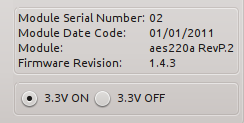
Fortunately turning off the supplies on an aes220 is very simple. If we open the aes220 Programmer, just below the Module information we can see two radio buttons. They both indicate the status of the 3.3V rail of the board and allow to turn it on or off.Turning on or off the supply is as easy as clicking the desired radio button. The status of the power supply being written to the EEPROM of the micro-controller the procedure does not have to be done each time the board is powered up.Note that because the 3.3V redistributed to the connectors is actually the same supply going to the IO pins of the FPGA turning it off means turning the FPGA GPIO off too (unless of course the 3.3V is provided by another board or an external source).Stacking up aes220 is as simple as turning off the 3.3V supply on all but one board and then connecting them together. Alternatively the 3.3V can be turned off on all the boards and provided externally. This can come handy if the sum of all the designs in the FPGA require more than the 1.5A that the running power supply can provide. To find out how much current your design use you will have to use Xilinx freely available Power Estimator (XPE) spreadsheet tool : http://www.xilinx.com/powerNote that we have to provide the 5V power supply via both USB cables. The 5V from the USB is not passed from one board to another so we need to either feed it to both boards via their own USB cable or we can use an external supply and feed both boards via one of the Vin and Ground pairs available on the connectors.
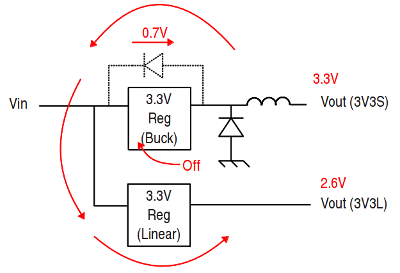
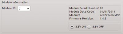
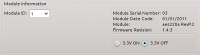
The boards will turn on with only one USB cable providing the supply because the 3.3V provided by the running regulator is passing from the output of the turned off regulator through it's body diode and reaches its input with a drop of .7V. The resulting 2.6V is enough to power up the remaining regulators and in turn the micro-controller. However the micro-controller is now running on 2.6V which is outside its specifications. There is no guaranty on how well it will run under these conditions and drawing more current or a change in temperature could get it to fail.If we take another look at the programmer we can see that a module ID. That module ID allows us to speak to one board or the other.Under ID 0 is the first board we plugged in and each board plugged there after will get an incrementing ID number.
Note also that the 3.3V rail can be turned on and off using two specific functions provided with the API. With API functions The board ID number can be recovered from the board serial number which is also printed on the PCB.