
Communicating with the aes220 High-Speed FPGA Mini-Module over the USB port
This write-up demonstrates the communication process between the PC and the aes220 module over the USB port. We make use of the FX2 interface and pipes in and out described in the module User Manual. We also will be using a short C program showing how to use the C routines described in the libaes220 API (www.support.aessent.com/aes220/apidocs/files/aes220_API-h.html)
The C program simply sends some bytes to the module, read them back and display them on a terminal console. The module stores the bytes coming in in its internal RAM and reads them out from the RAM when asked to produce them back.
To achieve this on the FPGA side we use the pipeIn and pipeOut entities, the device BRAM components, a counter to increase the RAM address and a minimum amount of logic for read / write access and loading the number of bytes to be handled into the counter. For demonstration we use two pipeIn entities to load a sixteen bit value into the counter.
The example shows how to set up the project using Xilinx ISE WebPACK (freely available from the Xilinx website www.xilinx.com). How to load the relevant files into the project and simulate the design using the provided simulation package for the aes220 module. Once simulated the example is compiled and downloaded into the device where it can be run using the C program provided. The C program is itself described so it can easily be used as a reference for future programs.
Verifying your setup:
Before trying to run this example it might be a good idea to verify your setup if you have never used the aes220 module before. You can do this by following the instructions in the previous post: Programming the aes220 High-Speed USB FPGA module using Xinlinx ISE WebPACK and the aes220 programmer which explains how to compile and run a short, basic example. That will help you ensure all the basic software requirements are in place on your PC.
Setting up the project
We will be using Xilinx ISE WebPACK tool in this example. The tool is freely available from Xilinx web site (see www.xilinx.com). For other tools, please, refer to the tool's own documentation, however the options shown here should apply whatever the tool used.
Note: only the options relevant to creating a project for the aes220 are shown here. For a deeper understanding of the different options of the Xilinx ISE WebPACK tool, please, refer to the Xilinx documentation.
Create a new project using the New Project Wizard and make sure to set the project settings to:
Family: Spartan 3A and Spartan 3AN
Device: XC3S200AN or XC3S400AN depending on which module you are developing for.
Package: FTG256
Speed: -4
Optionally you can change the VHDL Source Analysis Standard to VHDL-200X
Now add the source files to the project, you will need:
From the example directory:
- aes220_Loopback_Example_Testbench.vhd
- aes220_Loopback_Example.vhd
- simpleRam.vhd
- UpLoadCounter.vhd
Set the Association to Simulation for the testbench file and leave the rest to All.
From the utils directory:
- aes220_Library.vhd
- aes220_Package.vhd
- aes220_SimulationPackage.vhd
Set the Association to Simulation for the Simulation package and leave the rest to All.
From the ucf directory:
- aes220_RevA1_FX2_Interface.ucf
- aes220_RevA1_LED.ucf
Leave the Associations to Implementation for both files.
Once all the files have been added select the Simulation View for the Hierarchy window and highlight the Testbench file. In the Processes window below expend the ISim Simulator field and highlight the Simulate Behavioral Model field. Now click on the Process menu entry of the ISE Project Navigator main menu and select Process Properties. In the new Process Properties window change the Simulation Run Time from 1000ns to 4000ns.
The project is now ready to be simulated.
Simulating the example: what is going to happen?
Before launching the simulation we will have a look at the testbench and example files and describe in more details what is going to happen.
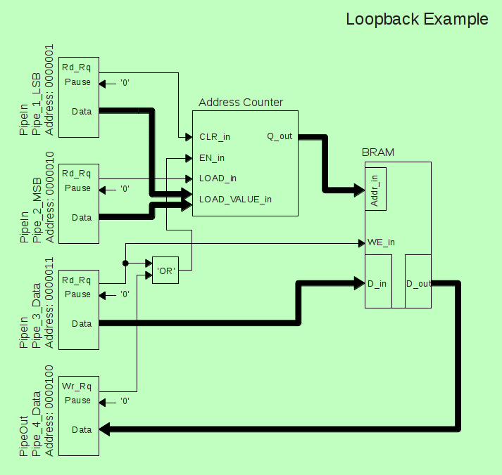
We want to write data coming from the PC to the RAM inside the FPGA using the USB pipes. In order to do that we link one pipe to the data input port of the RAM. To increase the RAM address as the data arrives we set a counter running on the address port of the RAM.
We could have set the counter running on the Read Required output of the pipe, however the USB communication is not guaranteed to be uninterrupted so we pre-load the counter with the number of bytes to be written to the RAM. There are different ways of achieving this but to show the flexibility of the pipes we are using two separate pipes to load the value into the counter. Pipe_1_LSB will reset the counter with its Read_Rq output and at the same time put the counter LSB value on its outputs. Pipe_2_MSB will put the counter MSB value on its outputs and at the same time assert the load input of the counter with its Read_Rq output.
Now that the counter is loaded with a value corresponding to the number of bytes to be written to the RAM all we have to do is to send the data via a third pipe (Pipe_3_Data) the Read_Rq output will enable the counter so the counter increment matches the data coming through the pipe.
Reading data from the RAM works in exactly the same way save that this time we are using a fourth pipe linked to the data output port of the RAM (Pipe_4_Data). Pipe_4 is an output pipe so this time it is its Write_Rq output which is linked to the enable pin of the counter.
In order to exercise and simulate our design we use a testbench file which, among other things, will replicate what the PC will have to do to communicate with the design in the FPGA.
Most of the testbench file is self explanatory but we will describe a few things here.
The clock period on the board is 20.8ns so, although not critical, we set it to be that in the test bench.
The channels (or pipes) addresses need to match the ones set in the example file. Note however that a pipe in in the FPGA is a pipe out on the PC side.
-- Channels addresses:
variable outChannel1_v : integer := 1;
variable outChannel2_v : integer := 2;
variable outChannel3_v : integer := 3;
variable inChannel_v : integer := 4;
We use byte arrays as data to be sent or received through the pipes, just like the C functions of the API, and after declaring them we fill the array to be written to the RAM in the FPGA with incrementing numbers using the index of a simple For loop. At the same time we set the array to be written into, when reading the data back from the RAM, to all zero.
for index in 0 to dataSize_v - 1 loopdata
Out_ar(index) := conv_std_logic_vector(index, 8);
dataIn_ar(index) := (others => '0');
end loop;
We assert and de-assert the reset signal inserting a wait statement in between covering some periods (one period would have been enough). Note that although the For loop has been placed between the assertion and release of the reset signal it in fact has no effect on the timing.
We then proceed with sending the data to the FPGA via the pipes in the following order:
- Send the LSB value for the number of bytes to be written to the RAM (which will also reset the counter) via pipe 1.
- Send the MSB value for the number of bytes to be written to the RAM (which will now load both values into the counter) via pipe 2.
- Send the data itself via pipe 3.
Now in theory we should send out the LSB and MSB values again to reset and load the counter before reading the data back from the RAM but since we are reading the same number of bytes back we will simply send the LSB value again which will have for effect to reset the counter (we don't need to re-load the values).
- Send the LSB value for the number of bytes to be written to the RAM (which will also reset the counter) via pipe 1.
- Read the data coming via pipe 4 (in channel).
Running the simulation
To launch the simulation double click on the Simulate Behavioral Model in the Processes window.
The ISim window will appear. By default there won't be many signals in the graph window. This is due to the nature of the test bench in this case. We have written bytes to arrays and effectively want to check the contents of the array in which the design should have written the contents of the RAM.
To do this we expand the aes220_loopback_example_testbench_ent field in the Instance and Processes window and select the :test_proc field. In the Objects window we will see the list of declared variables including the various arrays. The one we are interested in is datain_ar which should match dataout_ar, that is show in incrementing binary sequence from 0000 to 1111.
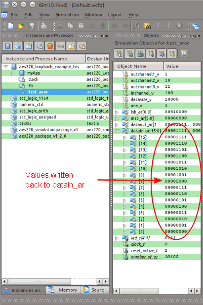
Fig 2. Results array
Implementing the design
Once the project as been simulated and the simulation gives the expected results it is time to implement the design in order to generate a configuration file for the FGPA.
To do this change the hierarchy view to Implementation, make sure the aes220_Loopback_Example_ent entity is selected and in the Processes window select Generate Programming File. Double clicking on this file would launch the creation of the programming file (via synthesis, mapping...) but before doing so ensure that the option Generate Binary Configuration File is selected in the Process Properties window (the Generate Programming File field needs to be selected in order for the window to display the relevant options). If this is the case double click on Generate Programming File.
The Synthesize-XST field in the Processes window should show a yellow warning triangle signalling there are some warnings to consider.
The Summary window will display the number of warning which should be 4 in our case. Clicking on the link will display the warnings. These should be about IP_in signal not being used and are nothing to worry about. There should also be one about the upper RAM addresses not being used and again can be ignored. The rest should be information messages.
The Implement Design and Generate Programming File fields of the Processes window should both display a green tick signifying that everything went smoothly.
The binary configuration file has now been created and can be found in the workspace directory of the project. It is the aes220_Loopback_Example_ent.bin file and is ready to be downloaded into the FPGA using the aes220 Programmer.
On the PC side
The aes220_LoopbackCmdLineExample.cpp file reproduces what was devised in the testbench file. The program once compiled will send the transfer size LSB value through pipe 1, the MSB value through pipe 2 and the data through pipe 3. Sending again the LSB value through pipe 1 to reset the counter in the FPGA it will then read the data coming back through pipe 4.
This is one example on how to use the pipes for communicating with the FPGA and shows how the C/C++ program relates to the testbench. Although future programs will vary widely from this example some things will still need to be present:
The Header file for the API library needs to be included and its path updated to where ever its location is on the system being used to compile the program., or better still, the path for the file added to the compiler search directories list. The library file itself (libaes220-x.x.x.dll or .so) needs to be added to the relevant directory (most likely the system32 directory on Windows and /usr/lib on Linux)
#include "../../../API/aes220_API.h"
// or #include <aes220_API.h> // if path added to the compiler list of searched directories
Before communicating with the module via the USB the device needs to be “opened” on the port. This is done with the aes220_Open(idx, vbs) C function in the following manner:
int idx = 0; // Module ID 0 if only aes220 module plugged in
int vbs = 3; // Messages verbosity, min = 0, max = 9
...
// Open the device and declare a handle pointing to it
aes220_handle *aes220_ptr = aes220_Open(idx, vbs);
If only one device is plugged in then it will automatically have an identification number idx of 0. If more then one device is plugged in (with the same VID/PID that is) then the idx number assigned to each module with increment with the order they are plugged in. If one module is subsequently unplugged the idx number for the other modules will not change unless the PC is power cycled. Note that you can use the function aes220_Get_Board_Info(...) to read the module serial number to link the idx number to the appropriate module.
The vbs switch is to determine the level of comments being recorded in the log file found in the same directory as the program executable. Select vbs= 0 for a minimum amount of log comment and 9 for a maximum, or anything in between (see the API documentation for more details).
Eventually you will have finish with using the device so remember to close the device down. That is terminate the USB communication with it. The communication can always be re-opened if needed:
// Close the device when no longer required
aes220_Close(aes220_ptr);
For more information on the different functions available look at the API documentation on the website: www.support.aessent.com/aes220/apidocs/files/aes220_API-h.html